Lab #1: Intro C Programming (100 pts)
There are three goals for this assignment:
- To get a taste for writing embedded code in the C programming language.
- To build a mental understanding for how GPIO works in the MSPMO+.
- To practice writing code for a custom PCB.
Due Date: Friday, January 23, 2026
We will do peer grading in class on Monday January 26, 2026, design and code will be assessed according to the rubric described below.
What should be turned in?
- A document in TXT or PDF format explaining your design. This might also include a diagram.
- Your commented code files.
Textbook
Chapter 2 of the the textbook has an extensive discussion of the GPIO interface.
The Task
You have been given a PCB designed by another engineer. The PCB is intended to function as a clock. In future labs, we will focus on ensuring precise timing; in this lab your goal is to correctly initialize the hardware and implement the passage of time.
The outer LED ring is intended to mark hours, and the inner ring is intended to mark minutes. On the PCB design, these are labeled LEDA12, LEDA1, …, LEDA11 (hours / outer ring) and LEDB12, LEDB1, …, LEDB11 (seconds / inner ring).
For this lab, you should change the state of the LEDs once per second. (The inner ring should circle in 12, and the outer ring in 12 * 12 = 144.) The delay() function delays in clock cycles. You should adjust the value of the delay to achieve this goal.
The full KiCad project is available in the git repository in the PCBs/Clock directory. Here is a screenshot of the block showing how the LEDs are connected to the MSPM0 pins.
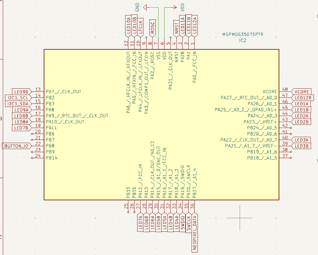
Note that each pin is labeled with its corresponding GPIO port and number (i.e., LED12A connects to PA0 and LED7B connects to PA11).
1. Initializing the hardware
As described in class, using simple GPIO requires correctly reseting and configuring several registers.
Specifically, the registers corresponding to the GPIOA and GPIOB modules, and those corresponding to
the IOMUX.
In class, we used the example of what needs to be configured in order to generate digital signals for the
pin labeled PA0. We described 3 basic steps:
- Reseting and powering on the GPIOA module
- Configuring the IOMUX
- Configuring the specific registers to set the value and enable channel 0
For PA0, the code looked like this:
/* 1. Reset and power on the GPIOA module */
*GPIOA->GPRCM.RSTCTL = 0xB100003;
*GPIOA->GPRCM.PWREN = 0x2600001;

/* 2. Configure the IOMUX */
IOMUX->SECCFG.PINCM[(IOMUX_PINCM1)] = (IOMUX_PINCM_PC_CONNECTED | ((uint32_t) 0x00000001));

/* 3. Enable channel 0 with a specified initial value of 1
*GPIOA->DOUTSET31_0 = (0x00000001);
*GPIOA->DOESET31_0 = (0x00000001);
Active HIGH or Active LOW?
Why are we initializing the value of the GPIO pin to 1 instead of 0. We want to initialize the pin so that the LED is inactive. If you open the full schematic, you’ll see on the LEDs page that the anode of the LED is connected to VCC and the cathode is connected to the GPIO pin. This means that if the pin is digital high (or about VCC), no current will flow, but if the pin is digital low (or about GND), current WILL flow and the LED will illuminate. So the LEDs are active in the LOW/ZERO state!
For each LED, there are TWO things that you need to know in order to make it light up (or turn off) and ONE ADDITIONAL thing you need to know to initialize it for functionality. What are these three things?
- What GPIO peripheral is it connected to? In the case of
PA0, which is connected to LEDA12 or the 12 o’clock hour hand outer ring, this isGPIOA. In the case of LED9B, the peripheral is alsoGPIOA. - What channel of the GPIO is it connected to? In the case of
PA0, manipulation of the LED is accomplished by manipulating the least significant bit in the 32 bit word mapped to GPIOA (bit 0). In the case of LED9B, it’s connected toPA7, so we manipulate the LED by manipulating the eighth bit (bit 7). - What IOMUX table entry controls that output channel? We learn this by looking at Table 6-2 in the
datasheet. For
PA0, this was entry 1. For LED7B (PA7), this is entry 14. Note that, because our code includes a critical header file (#include <ti/devices/msp/msp.h>), we have access to a predefined structure,IOMUX->SECCFG.PINCM[], and predefined constants for entries into this table like the constantIOMUX_PINCM1we used forPA0. NOTE. In CCS, you can right click on an identifier likeIOMUX_PINCM1and select “Go to Definition”, and it will open the header file where it’s defined. This is often a helpful way to learn about OTHER useful constants that might be predefined for you.
Checkpoint #0: Take a look at the schematic. Answer Question #1 for every pin. Do you need to reset
and power on both GPIOA and GPIOB?
A Lab1 project has been added to the git repository. It contains a new file, called initialize_leds.c
with a corresponding header file, initialize_leds.h. The function InitializeLEDs() has been prototyped
with the code for PA0. You should modify this function so that it properly completes the IOMUX, channel
initialization, and channel enabling for each LED on the board.
The IOMUX has a different register for each pin. In addition to enabling the pin (IOMUX_PINCM_PC_CONNECTED),
and setting the function (GPIO is function 0x1), there are a bunch of other settings we can configure for
each pin. However, the GPIO pin state (high or low) and output enable are configured by setting/clearing
individual bits in a 32 bit register.
Avoiding Clobbering
The MSPMO+ includes 3+ commands to manipulate the values of GPIO output enable and output value registers.
The simplest ones to understand are ones are DOE31_0 and DOUT31_0. These are the full 32 bit register with
one bit corresponding to the enable state / value for each channel. When writing these registers, you need
to be cautious about clobbering, so you should always read-manipulate-write, which you can also accomplish
with the OR-Equal (|=) and AND-Not-Equal (&= ~()) patterns we talked about in class.
Given that this is potentially always a concern, we have two more registerst that we can use. Writing the
DOESET31_0 register will only change values from a 0 to a 1, never from a 1 to a zero (it “sets” bits but
doesn’t clear them). So the command GPIOA->DOESET31_0 = 0x00000001; doesn’t actually change the enable
state of any of the channels except channel PA0. Simiarly GPIO->DOECLR31_0 = 0x00000001; would disable
channel PA0 but not affect any others. The commands with all zeros (GPIOA->DOESET31_0 = 0x00000000; and
GPIOA->DOECLR31_0 = 0x00000000;) have no effect.
Multiple Lines or One Line
Thus, in order to accomplish the channel output enable steps, you have a choice. You could do them one LED at a time, making sure not to clobber the values:
*GPIOA->DOE31_0 = LED12A_bit;
*GPIOA->DOE31_0 |= LED1A_bit; // notice the OR-Equals
*GPIOA->DOE31_0 |= LED2A_bit; // notice the OR-Equals
...
Equivalently, you could use the special DOESET31_0 registers
*GPIOA->DOESET31_0 = LED12A_bit;
*GPIOA->DOESET31_0 = LED1A_bit; // regular equals!
*GPIOA->DOESET31_0 = LED2A_bit; // regular equals!
...
BUT, nothing requires you to do this in separate lines. This is just as good:
*GPIOA->DOESET31_0 = LED12A_bit | LED1A_bit | LED2A_bit | ...;
The choice of which to do is really down to which one you can read and understand most clearly when you come back to maintain it later. (So comments are probably more important than actual code!)
The DOUT31_0 versus DOUTSET31_0 choice is identical for initializing the values of the GPIO pins.
2. Setting/clearing pins for individual LEDs in your code
Once the initialization code is written, you will need to manipulate the state of the LEDs in your
code. As we just discussed, for each GPIO port, this is done by carefully writing to the DOUT31_0
register or using the DOUTSET31_0 or DOUTCLR31_0 registers. Only writing the DOUT31_0 register
will allow you to modify the states of multiple LEDs in opposite directions in one instruction. (*)
3. State machine logic, data structures, etc
Once you are able to control the value of the LEDs as you want, you should implement the logic of the clock. You should adopt a state machine approach. A very simple variant has been mocked up in the lab template code, but you should feel free to make this more complex. For example, you might choose to implement states in a struct array, where each state’s entry specifies both the index of the next state and the value of the output. For another example, you could make the state a tuple instead of a single int.
Development process
A critical part of any embedded system development project is to work in stages. Ideally each stage tests specific portions of the code. Once a particular developmental stage is funcitoning correctly, you move on to the next, more complex stage. A key part of being an embedded developer is to identify the requirements for each of these stages and to plan your development process. By producing functional code at each step, you can be confident in the function of the final system.
For this project, we would suggest at least the following 3 preliminary stages.
- Programming the PCB. Wire up the PCB to the Launchpad debug section. Program the
blinkproject and ensure that you see the 12 o’clock LED (marked as D1 on the PCB) flashing. Completion of this stage will give you confidence that you understand how to wire up the PCB for programming and that it functions correctly. - Initializing the LEDs. Write your initialization code, and then set the value of all 24 of the LEDs to be on. This at least partially validates your initialization code and ensures that your PCB is functional in terms of LEDs being connected to known ports.
- Make the LEDs Flash in Sequence. Write code to go through a loop of all of the LEDs one at a time. This will ensure that you have correctly mapped LEDs to GPIO port/channels.
Grading Rubric
Here are a list of items which will be assessed as part of the grading of this lab.
- Design Document Present: Did the student submit a separate text or PDF file explaining their design approach?
- Diagram Included: Does the design document include a diagram (block diagram, state machine, or flow chart) visualizing the logic?
- State Machine Explanation: Does the documentation textually explain the states (e.g., “State A turns on LED 1…”)?
- Code Commentary: Are comments present in the C code explaining why specific hex values/registers are used?
- Power/Reset GPIO?: Does the code write to $GPRCM.RSTCTL$ and $GPRCM.PWREN$ for the appropriate GPIO module(s)?
- IOMUX Configuration: Is the IOMUX->SECCFG.PINCM register configured for the specific pins used (Function 1 + Connected)?
- Output Enable (DOE): Does the code enable the output driver for the relevant pins?
- Does the code use safe Read-Modify-Write logic or other techniques to avoid overwriting other potential pins on GPIOA?
- GPIO State Initialization: Does the initialization set the default output value appropriately so LEDs start OFF?
- Completeness: Does the initialization code address all 24 LEDs (Outer ring + Inner ring)?
- LED Activation Logic: To turn an LED ON, does the code use the appropriate values (i.e., 1 or 0)?
- Infinite Loop: Is the main logic wrapped in a while(1) or similar infinite loop structure?
- Data Structure/State Machine: Does code use a struct/array/switch-case rather than just linear if statements?
- Does the logic successfully manage the “Two Active Hands” requirement, ensuring that updating the Minute hand does not accidentally turn off the Hour hand (or vice versa)?
- Distinct Rings: Does the code attempt to control both the Outer Ring (Hours) and Inner Ring (Seconds)?
- Timing Delay: Is there a delay mechanism (e.g., __delay_cycles or loop) so changes are visible at 1 Hz?
- Sequence Wrap: Does the logic allow the sequence to wrap around (e.g., LED12 -> LED1)?