Lab #4: Thermodot PCB Design
There is just one goal for this assignment:
- To learn and carry out various aspects of printed circuit board design
What should be turned in?
- The EAGLE CAD .sch and .brd files for your design. (Canvas)
- The manufacturing files -
your-file-name.GBL(bottom layer),your-file-name.GML(board outline),your-file-name.GTL(top layer) andyour-file-name.TXT(drill locations). Don’t zip, compress, or otherwise combine these files! (Canvas)
What should be demo’d live?
- Your EAGLE CAD design, if desired.
Files are due Friday, February 9 at 7 AM
The early AM due date allows me to aggregate and submit files.
Designing a ThermoDot
In this part, we will put together most of the concepts from Part 1, creating a circuit with an
RGB LED and a temperature sensor. In order to do the rest of the assignment, you will need to
clone the ELEC327 reposistory from github (if you have
not done so yet). In the Labs/Lab3/Datasheets directory, you will find a data sheet for the
RGB LED (Digikey part
1516-1378-1-ND) and a
temperature sensor (Digkey part
296-25569-1-ND). Refer to the
data sheet for the RGB LEDs to choose current-limiting resistors.
The temperature sensor will be used with the built in analog to digital converter (ADC) module of the MSP430g2553. So the output pin will need to be connected to an appopriate input pin. We will discuss the ADC module further in future weeks. For now, you can see from the data sheet that there are eight pins (labeled A0-A7) which can be used for ADC input. I suggest you connect the temperature sensor to pin P1.0/A0. If you look at the temperature sensor’s data sheet, you’ll see that it is recommended that a capacitor be placed between the output line and ground – you may ignore this!
We will be using Eagle to design a PCB which contains the MSP430, RGB LED and a temperature
sensor. In the Labs/Lab4 directory, you will find a schematic which contains all but two
of the parts you will need. These are all part of the ELEC327 library, which is found in the
PCBs directory. You will need to create these 2 new parts - the RGB LED and the temperature
sensor. You will need to make both a schematic symbol and a package footprint.
Eagle comes with a good number of parts, but not all that you need. Start with the RGB LED. You should create a personal library for parts you make. Then, start with the “symbol”. Make sure to adequately labels the various connections. Pay special attention to the direction of current flow through each LED. Then you should create a “footprint”, referring to the data sheet for the spacing of the pads. Finally, combine the symbol and footprint so that the pins are connected to the right pads. Then, do the same for the temperature sensor. Note that for the temperature sensor, you can download an “Ultralibrarian” script from Digikey that will generate the symbol and footprint for you. Make sure you double check them, though!
Once you’ve made the RGB LED and the temperature sensor, add them to the schematic and connect them to the MSP430. We already have suggested P1.0/A0 for the temperature sensor. The RGB LED should be connected to PWM output pins connected to available Timer outputs. Remember to use 3 unique TA.x output pins – TA1.1, TA1.2, and TA0.1 (TA0.2 iff you’re not using the 20 pin device)!!!!
Next, then create a .brd file and route all of the connectionts. Keep in mind that the
battery package is solid and plastic, so you should not place any parts on top of it. One
solution is to put everything but the battery on one side of the PCB and the battery on the
other. Try to make the final board approximately 20-40 mm x 40 mm. Additionally, for this project,
PCB designs should be rectangular. After routing, check to make sure that it passes the
electrical rule check (ERC) and design rule check (DRC), using the DRC rules given in the
PCBS/AdvancedCircuitsBarebones.dru rule file.
After you place your components and route traces, please put your initials or some other identifying mark on the board on either the top or bottom copper layer (since this is a barebones process, there is no silkscreen).
When you’re finished, run the CAM job in PCBs/AdvancedBarebones.cam to create the necessary
files for manufacturing. We will submit a panel of the class’s designs for manufacturing, and
in a subsequent lab, you will assemble and test your PCBs. Thus, late submissions of this
portion of the assignment will mean that you lose points not only for this lab but also a
subsequent one!!!!
PCB Design Patterns and Anti-Patterns
A “Design Pattern” is an approach for a design task that will help you put small steps together into a full hole. When routing the traces on a PCB, straight lines, symmetry, and right angles are one possible pattern to follow. Note that this requires not just rotely following a rule - think about how you will make the routes while placing the components and deciding their rotation/orientation.
An “Anti-Design Pattern” is the opposite: rules of thumb that end up causing more problems than they solve. For the PCB example below, I imagine the student placing the components then thinking, “I will make the routes as straight as possible and introduce only minimal bends when necessary to avoid vias.” The result are a number of places where traces and vias are minimally separated, or parallel traces travel very closely (minimal separation) for a long distance. A piece of conductive junk ended up between two traces on this board, causing hours and hours of confused debugging.
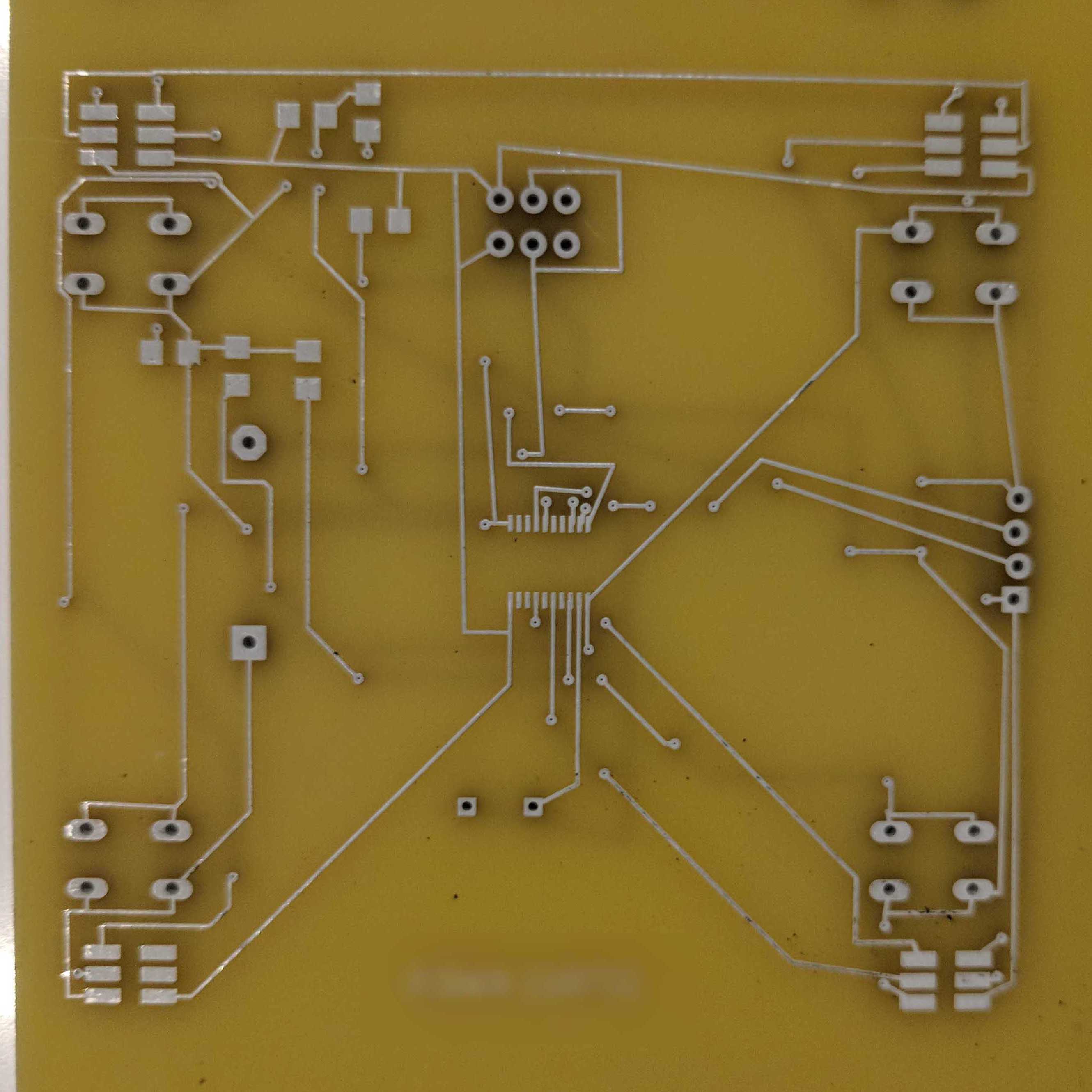
Anti-design PCB front
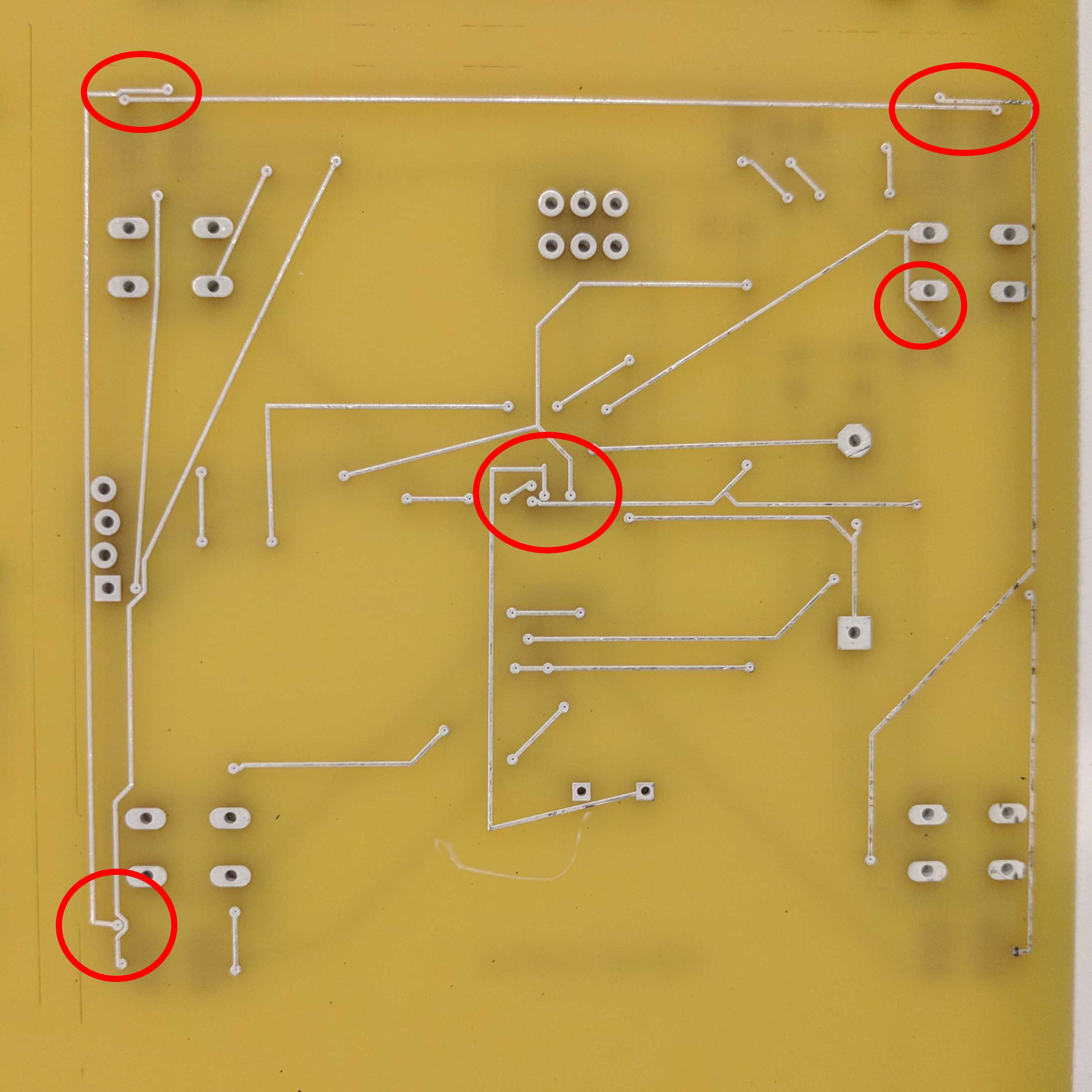
Anti-design PCB back
Upload the following PCB files to Canvas:
- the Eagle CAD .sch and .brd files
- manufacturing files -
your-file-name.GBL(bottom layer),your-file-name.GML(board outline),your-file-name.GTL(top layer) andyour-file-name.TXT(drill locations)
Please do NOT zip these, just upload them individually. If you do not follow this instruction I will deduct points from your score. (I use an automated script to extract these files.)